


MARKET INSIGHTS
Global EUV pellicle market was valued at USD 72 million in 2024 and is projected to reach USD 163 million by 2032, growing at a CAGR of 9.3% during the forecast period.
EUV pellicles are ultra-thin protective films used in semiconductor manufacturing to shield photomasks from contamination during extreme ultraviolet lithography processes. These specialized membranes maintain high light transmittance while preventing particulate contamination that could cause defects in semiconductor patterns. The technology has evolved from single-layer polysilicon structures to complex multi-layer designs combining molybdenum disilicide and silicon layers, achieving over 90% EUV transmittance.
Market growth is primarily driven by increasing adoption of EUV lithography in sub-7nm semiconductor manufacturing, where pattern sizes require exceptional precision. The transition to higher power EUV systems exceeding 500W has further increased demand for robust pellicle solutions. Key industry players including ASML, Mitsui Chemical, and S&S Tech are actively developing next-generation carbon nanotube (CNT) pellicles to meet evolving industry requirements for thermal stability and optical performance in advanced semiconductor fabrication processes.
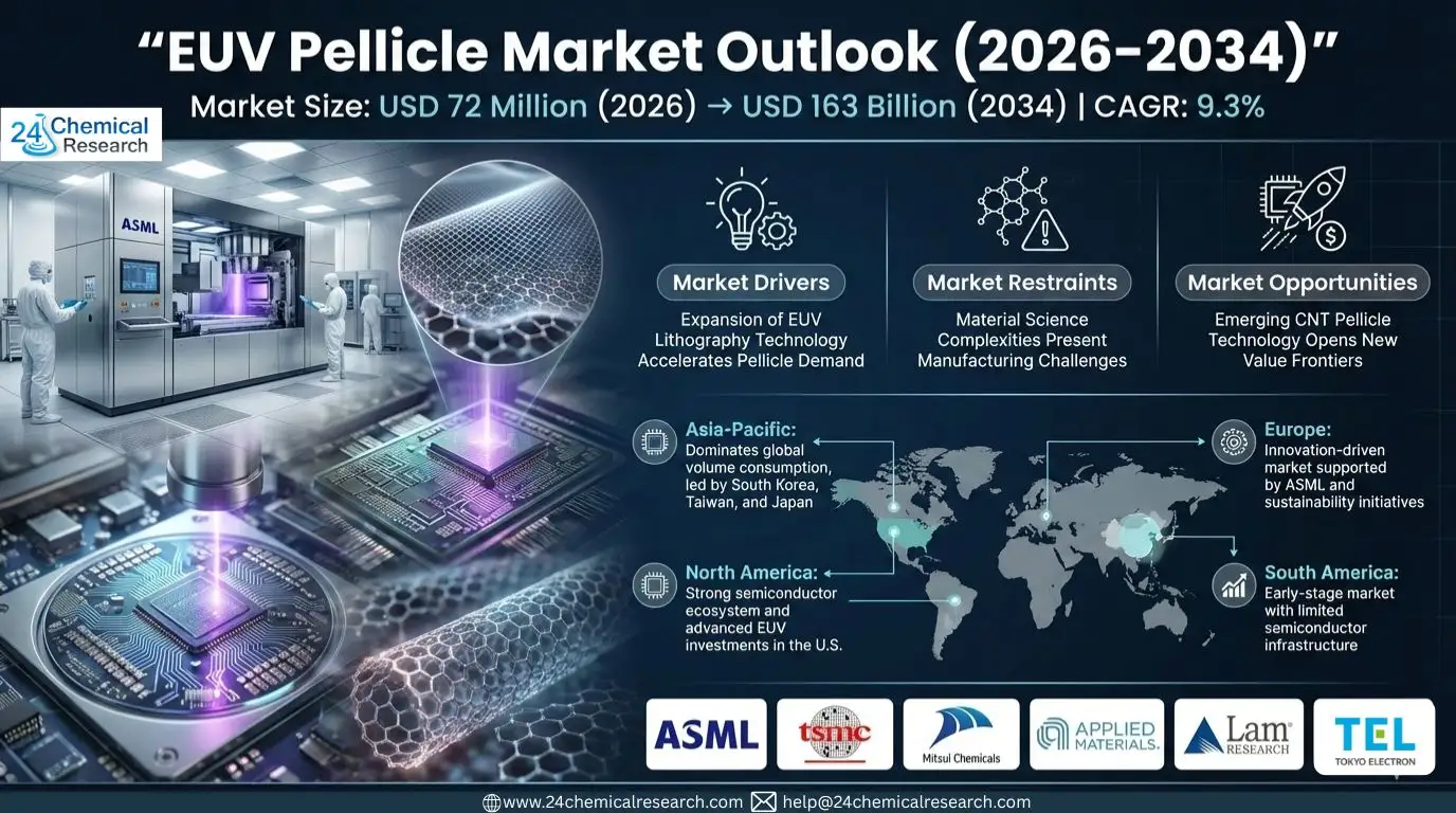
The Global EUV Pellicle Market was valued at USD 72 Million in 2024 and is projected to reach USD 163 Million by 2032, growing at a Compound Annual Growth Rate (CAGR) of 9.3% during the forecast period (2024–2032). This robust growth is being driven by the mass adoption of EUV lithography for sub-3nm chip nodes, increasing wafer production volume for AI and HPC applications, and a strategic industry push towards next-generation carbon nanotube (CNT) materials to enable high-NA EUV systems.
As the semiconductor frontier pushes towards angstrom-scale dimensions, the role of the pellicle as a critical contamination shield has never been more vital. In this blog, we profile the Top 10 Companies in the EUV Pellicle Industry—a specialized mix of chemical giants, semiconductor materials innovators, and integrated device manufacturers defining the standards for mask protection and yield enhancement in the world’s most advanced fabs.
🔟 10. Applied Materials, Inc.
Headquarters: Santa Clara, California, USA
Key Offering: Advanced material deposition solutions, pellicle R&D infrastructure
While not a direct pellicle manufacturer, Applied Materials is a pivotal enabler through its Materials Engineering capabilities. The company provides the thin-film deposition and atomic layer processing tools essential for developing and prototyping next-generation pellicle materials, including complex MoSi/Si multilayer stacks.
Innovation Initiatives:
- Providing enabling equipment for pellicle material R&D
- Collaborating with chemical suppliers on deposition process optimization
- Investing in materials discovery platforms for novel membrane solutions
Download FREE Sample Report:
EUV Pellicle Market – View in Detailed Research Report
9️⃣ 9. Canatu Oy
Headquarters: Helsinki, Finland
Key Offering: Carbon Nanotube (CNT) films for next-gen EUV pellicles
Canatu is a pioneer in carbon nanotube薄膜 technology, positioning itself as a key innovator for the future of EUV pellicles. Its proprietary CNT film technology offers a unique combination of high theoretical transmittance (>95%) and exceptional thermal and mechanical stability, making it a promising candidate for high-power EUV sources.
Innovation Initiatives:
- Strategic collaboration with imec on CNT pellicle development and integration
- Focusing on scalable manufacturing processes for defect-free CNT membranes
- Targeting qualification for high-NA EUV lithography tools
8️⃣ 8. Tokyo Electron Limited (TEL)
Headquarters: Tokyo, Japan
Key Offering: Coating and developing track systems, materials engineering expertise
TEL plays a crucial supporting role in the pellicle ecosystem through its coat/develop track systems used throughout the semiconductor patterning process. Its deep understanding of materials interaction, contamination control, and process integration provides valuable insights for pellicle performance and lifetime analysis within the fab environment.
Innovation Initiatives:
- Developing advanced surface preparation technologies
- Collaborating on pellicle contamination and defectivity studies
- Providing process integration knowledge for pellicle implementation
7️⃣ 7. Lam Research Corporation
Headquarters: Fremont, California, USA
Key Offering: Etch and deposition equipment, materials science expertise
Lam Research contributes to the pellicle value chain through its expertise in precision etch and atomic-level deposition. These capabilities are fundamental for creating and patterning the ultra-thin, uniform layers required for high-performance pellicles. Lam’s work on edge placement control and nanoscale material modification informs pellicle design for durability.
Innovation Initiatives:
- Leveraging atomic-scale processing knowledge for pellicle material innovation
- Exploring novel etch techniques for pellicle frame and membrane shaping
- Partnering with material suppliers on manufacturability challenges
6️⃣ 6. FST (Fine Semitech Corp.)
Headquarters: Hwaseong, South Korea
Key Offering: EUV pellicles, photomask blanks, semiconductor materials
FST is a South Korean specialty materials company that has emerged as a determined contender in the EUV pellicle space. While historically focused on photomask blanks, FST has actively developed its own EUV pellicle solutions, aiming to provide an alternative supply source and cater to the dense semiconductor manufacturing base in South Korea.
Innovation Initiatives:
- Developing proprietary pellicle membranes for high-transmittance applications
- Leveraging its photomask expertise for integrated pellicle-mask solutions
- Focusing on rapid qualification cycles with domestic foundry partners
Download FREE Sample Report:
EUV Pellicle Market – View in Detailed Research Report
5️⃣ 5. Taiwan Semiconductor Manufacturing Company (TSMC)
Headquarters: Hsinchu, Taiwan
Key Offering: In-house pellicle development and co-optimization for advanced nodes
As the world’s leading advanced logic foundry, TSMC is not just a consumer but a key developer of EUV pellicle technology. The company conducts significant in-house R&D on pellicles to co-optimize them with its proprietary process nodes, ensuring maximum yield and performance for its 3nm, 2nm, and beyond technologies.
Innovation Initiatives:
- Deep co-optimization of pellicle properties with specific process flows
- Developing custom pellicle solutions for unique integration schemes (e.g., backside power delivery)
- Setting the performance and reliability benchmarks for the entire industry
4️⃣ 4. S&S Tech Co., Ltd.
Headquarters: Hwaseong, South Korea
Key Offering: High-transmittance EUV pellicles, mask-related products
S&S Tech is a major force in the EUV pellicle market, known for achieving industry-leading 90.2% EUV transmittance with its multi-layer film technology. As a key supplier to major memory and logic manufacturers, the company is deeply integrated into the high-volume manufacturing supply chain, with a strong focus on yield, consistency, and supply security.
Innovation Initiatives:
- Continuous improvement of multi-layer film transmittance and durability
- Expanding production capacity to meet surging foundry and memory demand
- Developing pellicles optimized for high-NA EUV lithography requirements
3️⃣ 3. ASML Holding N.V.
Headquarters: Veldhoven, Netherlands
Key Offering: Integrated EUV pellicle solutions, technology licensing
ASML, as the sole provider of EUV lithography systems, holds a central and influential role. It originally developed pellicle technology in-house to ensure its scanners could be used in production. Today, ASML drives the ecosystem through technology licensing (e.g., to Mitsui Chemicals) and by setting the system-level specifications for pellicle performance, thermal budget, and mechanical compatibility.
Innovation Initiatives:
- Defining roadmaps for pellicle performance aligned with future EUV source power (600W+)
- Licensing core pellicle technology to accelerate ecosystem development
- Ensuring pellicle compatibility with next-generation High-NA EUV systems
2️⃣ 2. Samsung Electronics
Headquarters: Suwon, South Korea
Key Offering: Vertical integration of pellicle development for memory and foundry
Samsung, a leader in both memory and foundry logic, pursues a strategy of vertical integration for critical materials like EUV pellicles. The company invests heavily in internal pellicle development to secure its supply chain, reduce costs, and tailor the technology specifically for its aggressive DRAM scaling roadmap and advanced logic nodes.
Innovation Initiatives:
- Internal development of pellicles for both DRAM and logic applications
- Focus on pellicle durability for high-throughput memory production
- Strategic partnerships and investments in novel material startups
1️⃣ 1. Mitsui Chemicals, Inc.
Headquarters: Tokyo, Japan
Key Offering: Commercial EUV pellicles, Carbon Nanotube (CNT) film development
Mitsui Chemicals stands as the undisputed commercial leader in the EUV pellicle market. Through an exclusive license of the core technology from ASML, Mitsui has scaled production and become the primary supplier to the global semiconductor industry. The company is now pioneering the next leap with significant investments in Carbon Nanotube (CNT) pellicle technology, aiming to maintain its leadership through the transition to more demanding lithography eras.
Innovation Initiatives:
- Mass production of current-generation polysilicon and multi-layer pellicles
- Aggressive R&D and planned production facility for CNT-based pellicles
- Continuous work to improve transmittance, defect density, and operational lifetime
Get Full Report Here:
EUV Pellicle Market – View in Detailed Research Report
🔬 Outlook: The Future of EUV Pellicles is Smarter and Multi-Material
The EUV pellicle market is undergoing a foundational shift. While multi-layer silicon-based films dominate today’s high-volume manufacturing, the industry is investing heavily in nano-engineered materials like carbon nanotubes, advanced deposition techniques, and AI-driven defect inspection to meet the unprecedented demands of the angstrom era.
📈 Key Trends Shaping the Market:
- Material transition from multi-layer Si/MoSi to Carbon Nanotube (CNT) films for high-NA EUV
- Increasing vertical integration by major IDMs and foundries for supply chain security
- Rise of application-specific pellicle designs optimized for logic, memory, or advanced packaging
- Tighter integration of pellicle performance data with fab-wide yield management systems
Get Full Report Here:
EUV Pellicle Market – View in Detailed Research Report
The companies listed above are not only protecting the world’s most advanced photomasks—they’re enabling the continuation of Moore’s Law and the creation of the next generation of AI, automotive, and connected devices.
- Top 10 Companies in the Global Electrochromic (EC) Windows Market (2026) - April 2, 2026
- Top 10 Companies in the South Korea Non-Woven Glass Fiber Prepreg Industry (2026): Market Leaders Powering Advanced Composites - April 2, 2026
- Top 10 Companies in the Conducting Polyaniline Industry (2028): Pioneers Powering Advanced Electronics and Sustainable Growth - April 2, 2026